CYRANNUS HE100 / HE300
Precision for heteroepitaxial diamond synthesis
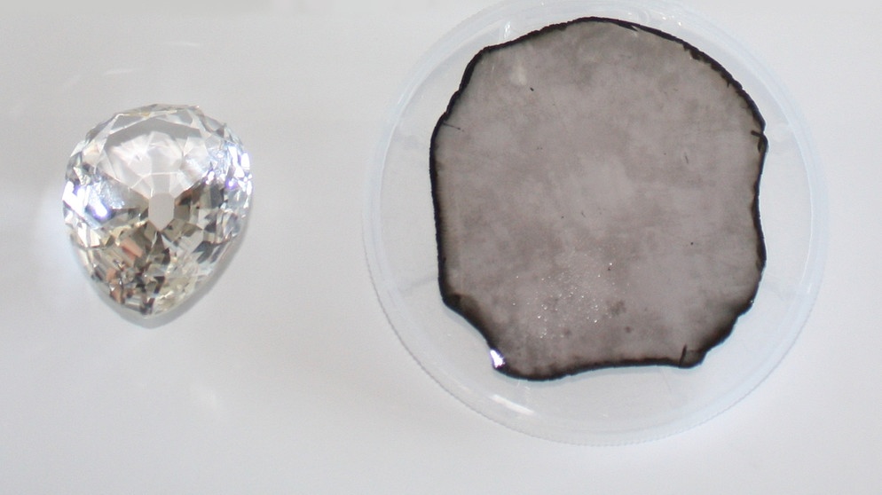
Specially developed for high-precision heteroepitaxial diamond growth on wafers (HE100 for up to 100 mm, HE300 for up to 300 mm). Essential for state-of-the-art electronics and photonics.
Tailor-made for heteroepitaxial diamond growth on wafers
Specially developed for advanced heteroepitaxial diamond synthesis, it enables the production of high-quality diamond layers on various foreign substrates, including iridium (Ir) and silicon (Si) wafers, with high precision and uniformity. Crucial for next-generation semiconductor devices and special optical components.
Heterogeneous diamond synthesis on wafers up to 100 mm (HE100) and 300 mm (HE300).
Growth of highly oriented diamond layers.
Deposition on various substrate materials.
- Highly homogeneous diamond coatings
- Precise control of layer thickness/properties
- Exceptional crystal quality
- Optimised for specific substratesScalable production with HE300
Benefits of the CYRANNUS HE-Serie
- High-quality diamond coatings: Superior films for state-of-the-art devices.
- Efficient substrate utilisation: Maximum utilisation of expensive wafer materials.
- Reproducible results: Consistent film properties for reliable manufacturing.
- Scalable production: HE300 offers capacity for industrial wafer processing.
- Customised properties: Control of material properties for specific device requirements.
Important applications of heteroepitaxial diamond synthesis
- Semiconductor materials for high-performance electronics
- Optoelectronic components
- MEMS sensors
- UV detectorsHeat dissipation elements
Used, for example, at the University of Augsburg in the development of novel semiconductor materials.